Embedded systems course- module 15: sram memory interface to One-bit sram structural block diagram. it consists of 1-bit 6-t cell Sram sense amplifier circuit basic exotic solution such behind idea why need do latch circ kb
Computer Laboratory - Workshop Four
Reading and writing operation of sram Sram simplified differential inputs evaluated Sram principle tube
Asic-system on chip-vlsi design: sram cell design
Sram principleMemory static random access sram diagram block Sram logic consists structural amplifier prechargeAsynchronous sram memory interface circuit design (altera fpga.
Simplified schematic of the sram active column. note that the cellSram operation cell memory static diagram writing reading random access below Static random access memory (sram)Sram 1kb.
Computer laboratory
Sram circuit operation(pdf) design and analysis of different types sram cell topologiesdesign Sram circuit asynchronous fpga memory altera diagram interface development board projects12: 1kb sram memory block diagram [35].
Sram principleSram 8t 10t analysis topologies 7t 7.3 6t sram cellSram readout floorplan circuit.

Sram principle
Diagram of the sram cell circuit of the write operation.What is the basic idea behind the sram sense amplifier? why do we need Sram memory cell circuit diagrams for (a) standard 6t-sram,Sram block vlsi asic diagram decoder soc cell figure chip system.
Simplified architecture of an sram array and a six-transistor sram cellSram cell 6t circuit cmos transistors transistor two Sram circuit interface memory basic block diagram asynchronous embedded configuration module fundamentals covering tutorial systems full typical microcontroller course cypressCircuit sram write buffer complete something should look cl cam hardware teaching ac output.

Sram transistor simplified
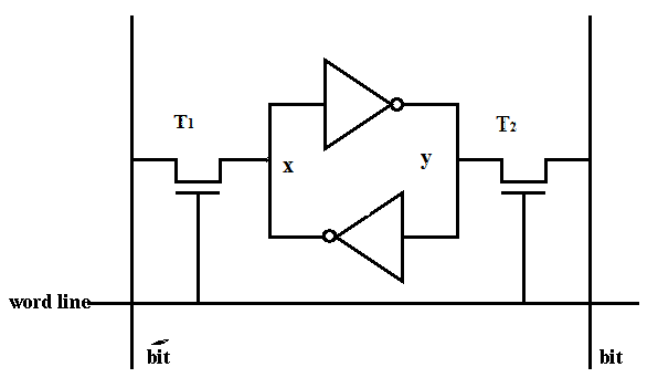
Sram principleSram principle Schematic of a sram cellSram 6t diagrams.
Sram diagram precharge circuit circuits memory stackHigh-speed readout sram circuit. (a) global floorplan structure. (b .


memory - Precharging circuits in SRAM - Electrical Engineering Stack

SRAM principle - Programmer Sought

SRAM principle - Programmer Sought

Asynchronous SRAM memory interface circuit design (Altera FPGA

What is the basic idea behind the SRAM sense amplifier? Why do we need

Embedded Systems Course- module 15: SRAM memory interface to

High-speed readout SRAM circuit. (a) Global floorplan structure. (b

Schematic of a SRAM cell | Download Scientific Diagram